Zero-Trust Security Revolution: Verify Everything Always
Zero-Trust Security Revolution: Verify Everything Always
How Ray Tracing Hardware Revolutionized Real-Time Graphics

DNA Data Storage: Encoding Humanity's Digital Future
How Gaming GPUs Became the Engine of the AI Revolution
RISC-V Revolution: Open-Source Chips Challenge Intel & ARM
Why Quantum Computers Can't Stay Quantum: The Decoherence Crisis
TL;DR: Spintronics harnesses electron spin rather than charge to create faster, more energy-efficient computing. Already powering hard drives and emerging MRAM chips, the technology could slash processor power by 80% and enable neuromorphic AI hardware by 2030.
In 2025, a technology once confined to physics laboratories is quietly reshaping how the world stores and processes information. Spintronics harnesses not the electrical charge of electrons but their intrinsic quantum property called spin, opening pathways to computers that operate faster, cooler, and more efficiently than anything silicon can deliver. While most people have never heard the term, spintronic devices are already inside millions of laptops, smartphones, and data centers. The question is no longer whether spintronics works, but how quickly it will leapfrog the half-century reign of conventional electronics.
Every electron carries two distinct properties: charge and spin. Traditional electronics has built an empire on charge alone, shuttling electrons through transistors to represent zeros and ones. Spin, by contrast, is an intrinsic form of angular momentum that makes each electron behave like a tiny bar magnet, pointing either "up" or "down." Unlike charge, which dissipates as heat when electrons collide with atoms, spin can flip almost instantaneously and persists without external power, a property physicists call non-volatility.
That difference might sound academic, but it translates into transformative performance. Conventional memory chips leak power constantly because they must refresh stored data thousands of times per second. Spintronic memory, by anchoring information in the magnetic orientation of electron spins, holds data indefinitely with near-zero leakage. Early prototypes have demonstrated write speeds under 50 nanoseconds while consuming up to 80% less power than conventional cache memory.
The breakthrough came in 1988 when physicists discovered giant magnetoresistance, earning them the 2007 Nobel Prize and unlocking the first commercial spintronic devices.
Yet for decades, manipulating spin remained a laboratory curiosity. The breakthrough came in 1988 when physicists Albert Fert and Peter Grünberg independently discovered giant magnetoresistance, or GMR, a phenomenon in which the electrical resistance of layered magnetic films changes dramatically when electron spins align. That discovery earned them the 2007 Nobel Prize in Physics and unlocked the first commercial spintronic devices.
The first real-world application of spintronics arrived in 1997, when IBM introduced GMR-based read heads in hard disk drives. By exploiting the spin-dependent scattering of electrons in multilayer magnetic films, these sensors could detect the microscopic magnetic fields of individual data bits with unprecedented sensitivity. The result was a sudden leap in storage density and speed, enabling hard drives to pack more information into smaller spaces.
GMR works through a simple but elegant mechanism. Picture two layers of ferromagnetic material separated by a thin non-magnetic spacer, typically copper or chromium. When the magnetizations of both layers point in the same direction, electrons with matching spins flow smoothly through the stack, encountering low resistance. Flip one layer's magnetization anti-parallel to the other, and minority-spin electrons scatter violently at each interface, driving resistance upward. In laboratory conditions, resistance can change by 50% at cryogenic temperatures, though practical devices at room temperature see shifts closer to 3-20%.

By 2025, virtually every hard drive on the planet uses some form of spintronic sensor. The technology that won a Nobel Prize has become so ubiquitous it's invisible. But GMR was only the beginning. Researchers soon realized that if electron spin could sense magnetic fields, it could also store information. That insight gave birth to magnetoresistive random-access memory, or MRAM, a technology that promises to combine the speed of SRAM, the density of DRAM, and the non-volatility of flash storage all in one chip.
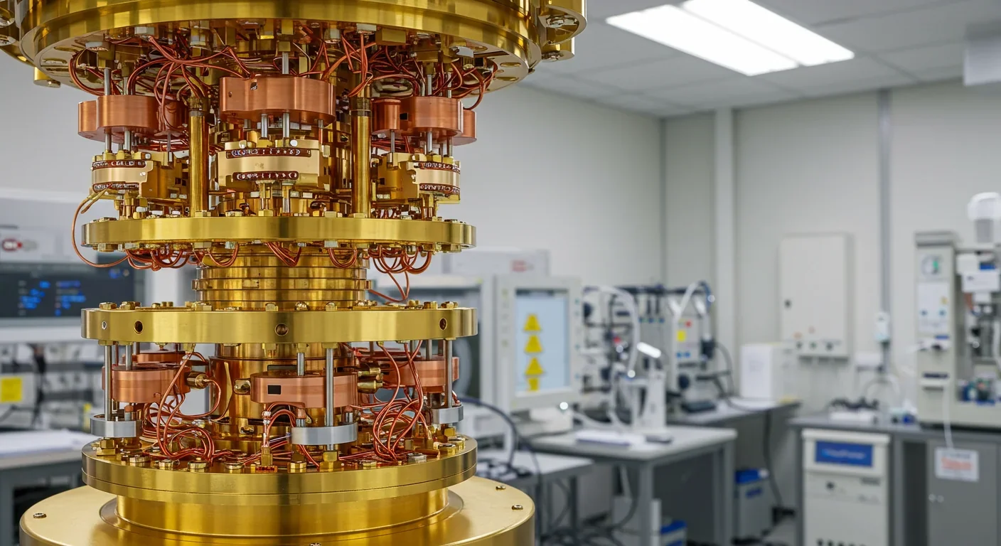
Unlike DRAM, which stores charge in capacitors that leak and fade, MRAM uses magnetic tunnel junctions to lock data in place. Each memory cell consists of two magnetic layers separated by an ultra-thin insulating barrier, often magnesium oxide. When the layers' magnetizations align, electrons can tunnel through the barrier easily, representing a logical "1." When anti-aligned, tunneling probability drops, signaling a "0." Because the magnetic state persists without power, MRAM chips retain data through power cuts, crashes, or even exposure to radiation.
That last property has made MRAM a favorite in extreme environments. Everspin Technologies, the first company to commercialize spintronic memory, has deployed MRAM in Airbus aircraft and BMW motorcycles, where reliability under heat stress and cosmic-ray bombardment is non-negotiable. Automotive systems, industrial controllers, and aerospace electronics all face conditions that would scramble conventional memory; MRAM shrugs them off.
"Spin-transfer torque allows a spin-polarized current to directly flip a magnet's orientation by transferring angular momentum from flowing electrons to the magnetic layer itself, no external field required."
— John Slonczewski's 1996 theoretical prediction
Yet early MRAM had a critical flaw. Writing data required generating magnetic fields strong enough to flip the storage layer's magnetization, which consumed significant power and limited how small the cells could shrink. The solution arrived in the form of spin-transfer torque, or STT, a phenomenon predicted by physicist John Slonczewski in 1996. STT allows a spin-polarized current to directly flip a magnet's orientation by transferring angular momentum from flowing electrons to the magnetic layer itself, no external field required.
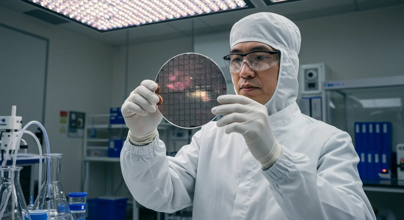
STT-MRAM devices are faster, denser, and more energy-efficient than their field-switched predecessors. Sony built the first working 4 kb STT memory in 2005, and by 2012, Everspin had released a 64 Mb DDR3 module. Intel demonstrated STT-MRAM for processor cache in 2019, and major semiconductor firms including Samsung, Qualcomm, and Toshiba are all racing to integrate spintronic memory into next-generation chips.
Why does any of this matter? Because conventional electronics is running into a wall. Every year, data centers consume more electricity, smartphones demand larger batteries, and chip designers wrestle with heat dissipation that limits how many transistors can fit on a die. The culprit is Joule heating: whenever electrons move through a resistive material, they shed energy as waste heat. In a world where Google alone uses as much energy annually as the entire city of San Francisco, even small efficiency gains compound into massive savings.

Spintronics offers a way out. Because spin currents can propagate with minimal charge flow, devices based on spin-transfer torque can theoretically approach 100% efficiency under ideal conditions, eliminating Joule losses entirely. Real-world devices won't hit that limit, but even partial reductions in switching energy make a difference. Magnetic tunnel junctions in current research prototypes operate at 10-100 femtojoules per bit, a tiny fraction of the energy conventional transistors require.
Add non-volatility into the mix and the savings multiply. Computers spend enormous power keeping DRAM refreshed and SRAM energized. Replace those with MRAM, and idle systems could shut down memory entirely without losing state. Mobile devices would wake instantly from deep sleep, servers could cut standby power to near zero, and "instant-on" computing would become the norm rather than the exception.
Spintronics enables capabilities that charge-based electronics cannot match: magnetic states can represent more than binary logic, and spin currents can process and store data in the same physical location.
Yet spintronics also enables capabilities that charge-based electronics simply cannot match. Because magnetic states can represent more than binary logic—through techniques like skyrmion manipulation or multi-level storage—spintronic devices can pack more information per cell. And because spin currents interact directly with magnetic domains, spintronic circuits can process and store data in the same physical location, blurring the line between memory and logic in ways that mirror how biological neurons work.
For all its promise, spintronics faces stubborn obstacles. The most immediate is switching current. STT-MRAM requires a pulse of spin-polarized electrons strong enough to overcome a magnetic layer's thermal stability, ensuring that random heat fluctuations don't accidentally flip bits. But too much current heats the device, shortens its lifespan, and consumes the very power spintronics is supposed to save. Researchers have spent two decades engineering materials—particularly MgO tunnel barriers—that boost tunnel magnetoresistance while lowering the threshold current, but current density remains too high for many cost-sensitive applications.
Material challenges run deeper. Conventional electronics enjoys the advantage of mature, billion-dollar fabrication ecosystems built around silicon, copper, and aluminum. Spintronics demands exotic combinations: ferromagnetic alloys like cobalt-iron-boron, rare-earth elements for perpendicular magnetic anisotropy, and atomically precise interfaces between magnetic and non-magnetic layers. Small variations in thickness or roughness can destroy spin coherence, the delicate quantum state that allows spins to propagate without flipping randomly. In metals, spin lifetimes rarely exceed one nanosecond, limiting how far spin information can travel before it decoheres.
Semiconductors offer longer spin lifetimes—researchers have demonstrated persistent spin helices in gallium arsenide that last more than a nanosecond, thirty times longer than earlier efforts—but integrating magnetic materials with semiconductor logic remains an unsolved puzzle. You can't simply swap a spintronic memory cell into a conventional processor and expect it to work. The interfaces, voltages, and timing all differ. Hybrid chips that marry CMOS logic with spintronic memory are emerging, but they require new design tools, testing protocols, and manufacturing workflows.
If spintronics were only about memory, it would still be revolutionary. But the field's long-term potential lies in rethinking computation itself. Researchers are exploring spintronic logic gates that perform calculations directly using spin currents, bypassing charge transport entirely. Spin valves and domain-wall devices can act as transistors, switches, and even oscillators, opening the door to circuits that blend memory and processing in a single device.
One of the most intriguing directions is neuromorphic computing, where hardware mimics the architecture of biological brains. Neurons communicate through synapses that strengthen or weaken based on activity, a property called plasticity. Spintronic devices exhibit analogous behavior: the resistance of a magnetic tunnel junction can change gradually as it accumulates pulses, effectively "learning" patterns in the input. By arranging arrays of magnetic tunnel junctions or skyrmion-based cells, researchers are building chips that perform tasks like image recognition or speech processing with far less power than conventional neural networks.
"Skyrmion-based devices operate at energies as low as 0.3-1 femtojoule per event, with switching speeds approaching 100 meters per second and footprints below 100 nanometers."
— Research findings on magnetic skyrmions
Skyrmions—tiny, swirling vortices of magnetization that behave like particles—represent one frontier of spintronic logic. These structures are topologically protected, meaning they resist random disruptions, and can be moved, created, and annihilated with minute currents. Skyrmion-based devices operate at energies as low as 0.3-1 femtojoule per event, with switching speeds approaching 100 meters per second and footprints below 100 nanometers. In principle, a chip built from skyrmion logic could outperform CMOS in speed, density, and efficiency simultaneously.
Antiferromagnetic spintronics offers another leap. Unlike ferromagnets, where all magnetic moments align in one direction, antiferromagnets have neighboring moments that point in opposite directions, canceling out to produce zero net magnetization. That makes them immune to stray magnetic fields and enables terahertz-scale switching, potentially a thousand times faster than conventional spintronic devices. Researchers are still learning how to read and write antiferromagnetic states reliably, but early experiments suggest that antiferromagnetic materials could form the basis for ultrafast, high-density memory and logic.
Two-dimensional materials add yet another dimension. Graphene, transition-metal dichalcogenides, and van der Waals heterostructures can host exotic spin textures with exceptionally long coherence times. By stacking atomically thin magnetic and non-magnetic layers, scientists are building devices that exploit quantum phenomena like the Dzyaloshinskii-Moriya interaction to stabilize skyrmions and control spin-orbit torques with unprecedented precision.
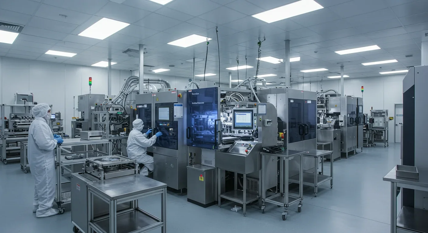
Spintronics is no longer a niche academic pursuit. Governments, universities, and corporations worldwide are pouring resources into spin-based technologies, driven by the recognition that whoever masters spintronics will shape the next era of computing. In Europe, institutions like the University of Lorraine have built specialized fabrication facilities—such as an 80-meter vacuum "Tube" that allows end-to-end production of spintronic prototypes in a single clean environment. That infrastructure bridges the gap between research and manufacturing, enabling rapid iteration on new device concepts.
Asian firms are betting heavily on MRAM commercialization. Samsung has integrated STT-MRAM into embedded memory roadmaps, targeting automotive and IoT markets where non-volatility and endurance matter more than raw speed. Toshiba and Sony continue to refine spin-transfer torque techniques, while Chinese research institutes are exploring antiferromagnetic and 2D spintronic materials as potential leapfrog technologies. Japan, home to early STT-MRAM patents and the first working prototypes, remains a hub for spintronic innovation.
While Silicon Valley pushes incremental transistor scaling, researchers in Europe and Asia are building the manufacturing infrastructure for a post-silicon world powered by electron spin.
In the United States, Intel's demonstration of STT-MRAM for processor cache signals that major chipmakers see spintronic memory as more than a niche product. Qualcomm has explored MRAM for mobile applications, where power efficiency directly translates to battery life. Startups and university spin-offs are experimenting with spintronic sensors for everything from biomedical diagnostics to quantum computing interfaces, betting that the same physics enabling memory can unlock new sensing modalities.
So when will spintronics truly replace silicon? The honest answer is that it won't, at least not entirely. Conventional CMOS transistors excel at logic operations, and decades of optimization have made them extraordinarily cheap and reliable. Spintronics is not about erasing the past but augmenting it. The most likely near-term trajectory involves hybrid systems where spintronic memory sits alongside silicon logic, each doing what it does best.
By 2030, expect to see MRAM in mainstream consumer electronics. Smartphones with instant-on capability, laptops that resume from hibernation in milliseconds, and embedded systems that survive power outages without data loss are all within reach. Automotive and industrial sectors will adopt spintronics faster because they value robustness and low power over cutting-edge performance. Data centers, perpetually hunting for energy savings, will deploy spintronic cache and storage-class memory wherever the economics make sense.
Further out, spin logic and neuromorphic chips could redefine what computation looks like. Machine learning accelerators built from spintronic neurons might train models with a fraction of the energy GPUs consume today. Quantum computers, which already manipulate electron and nuclear spins, could integrate spintronic control circuitry to improve coherence and reduce overhead. Wearable and implantable devices, where power budgets measure in microwatts, will benefit enormously from non-volatile, ultra-low-energy memory.
The transition won't be seamless. Every new technology faces a chasm between laboratory success and mass production. Fabrication yields must climb, costs must fall, and engineers must learn to design around spintronics' quirks. Standards for testing, reliability, and compatibility are still emerging. But the trajectory is clear. Conventional electronics, for all its triumphs, is approaching fundamental limits. Spin offers a path forward.
For professionals in technology, understanding spintronics is becoming as essential as understanding transistors once was. Electrical engineers designing next-generation processors need to account for hybrid memory architectures. Materials scientists developing new alloys and heterostructures will find eager customers in the semiconductor industry. Software developers optimizing for non-volatile memory can unlock performance gains that hardware alone cannot deliver.
Investors watching the semiconductor sector should note that spintronics is not speculative anymore. Companies like Everspin and Crocus Technology are shipping products today. Established giants like Samsung and Intel have publicly committed to spintronic roadmaps. The question is not whether spintronics will succeed but which companies and technologies will dominate the market.
"Spintronics is, in short, the daughter of electronics, not its sister. A daughter is often more advanced than its parent."
— Roman Morgunov, The History and Future of Spintronics
For policymakers, spintronics represents both an opportunity and a challenge. Nations that build robust spintronic research ecosystems and manufacturing capacity will capture high-value segments of the global electronics supply chain. Those that lag risk becoming permanent importers of critical technology. Investment in education, infrastructure, and public-private partnerships today will determine competitive positioning for decades.
And for individuals simply trying to understand where technology is headed, spintronics offers a rare glimpse of a genuine paradigm shift. Not an incremental improvement, not a marketing buzzword, but a fundamentally different way of encoding, moving, and processing information. The electrons flowing through your devices carry more than charge. They carry spin. And soon, they'll carry the future.

Lunar mass drivers—electromagnetic catapults that launch cargo from the Moon without fuel—could slash space transportation costs from thousands to under $100 per kilogram. This technology would enable affordable space construction, fuel depots, and deep space missions using lunar materials, potentially operational by the 2040s.

Ancient microorganisms called archaea inhabit your gut and perform unique metabolic functions that bacteria cannot, including methane production that enhances nutrient extraction. These primordial partners may influence longevity and offer new therapeutic targets.
CAES stores excess renewable energy by compressing air in underground caverns, then releases it through turbines during peak demand. New advanced adiabatic systems achieve 70%+ efficiency, making this decades-old technology suddenly competitive for long-duration grid storage.

Human children evolved to be raised by multiple caregivers—grandparents, siblings, and community members—not just two parents. Research shows alloparenting reduces parental burnout, improves child development, and is the biological norm across cultures.

Soft corals have weaponized their symbiotic algae to produce potent chemical defenses, creating compounds with revolutionary pharmaceutical potential while reshaping our understanding of marine ecosystems facing climate change.

Generation Z is the first cohort to come of age amid a polycrisis - interconnected global failures spanning climate, economy, democracy, and health. This cascading reality is fundamentally reshaping how young people think, plan their lives, and organize for change.
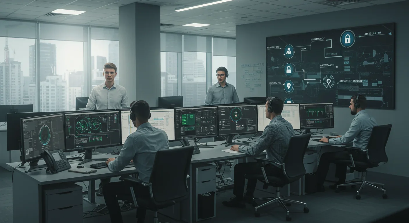
Zero-trust security eliminates implicit network trust by requiring continuous verification of every access request. Organizations are rapidly adopting this architecture to address cloud computing, remote work, and sophisticated threats that rendered perimeter defenses obsolete.

Loading featured articles...