AI Training Data Copyright Crisis: Lawsuits & Solutions

AI Training Data Copyright Crisis: Lawsuits & Solutions

Prompt Engineering: The Essential AI Literacy for 2025

AI Bias Crisis: How Machines Amplify Human Prejudice

Quantum Computing Revolutionizes Climate Modeling in 2025

Decentralized Identity: Own Your Digital Self Without Big Tech

No-Code AI Platforms: The Future of Machine Learning
TL;DR: Memristors—nanoscale devices that remember their electrical history—are poised to collapse the boundary between memory and computation, enabling AI chips that are 47× faster and 73× more energy-efficient than GPUs. Predicted in 1971 and realized in 2008, they promise instant-on devices, in-memory neural networks, and data centers that slash power by 90%. Yet manufacturing challenges, device variability, and ecosystem integration hurdles mean widespread adoption may not arrive until 2030–2035. The stakes are existential: memristors could democratize edge AI or concentrate control in those who own the foundries.
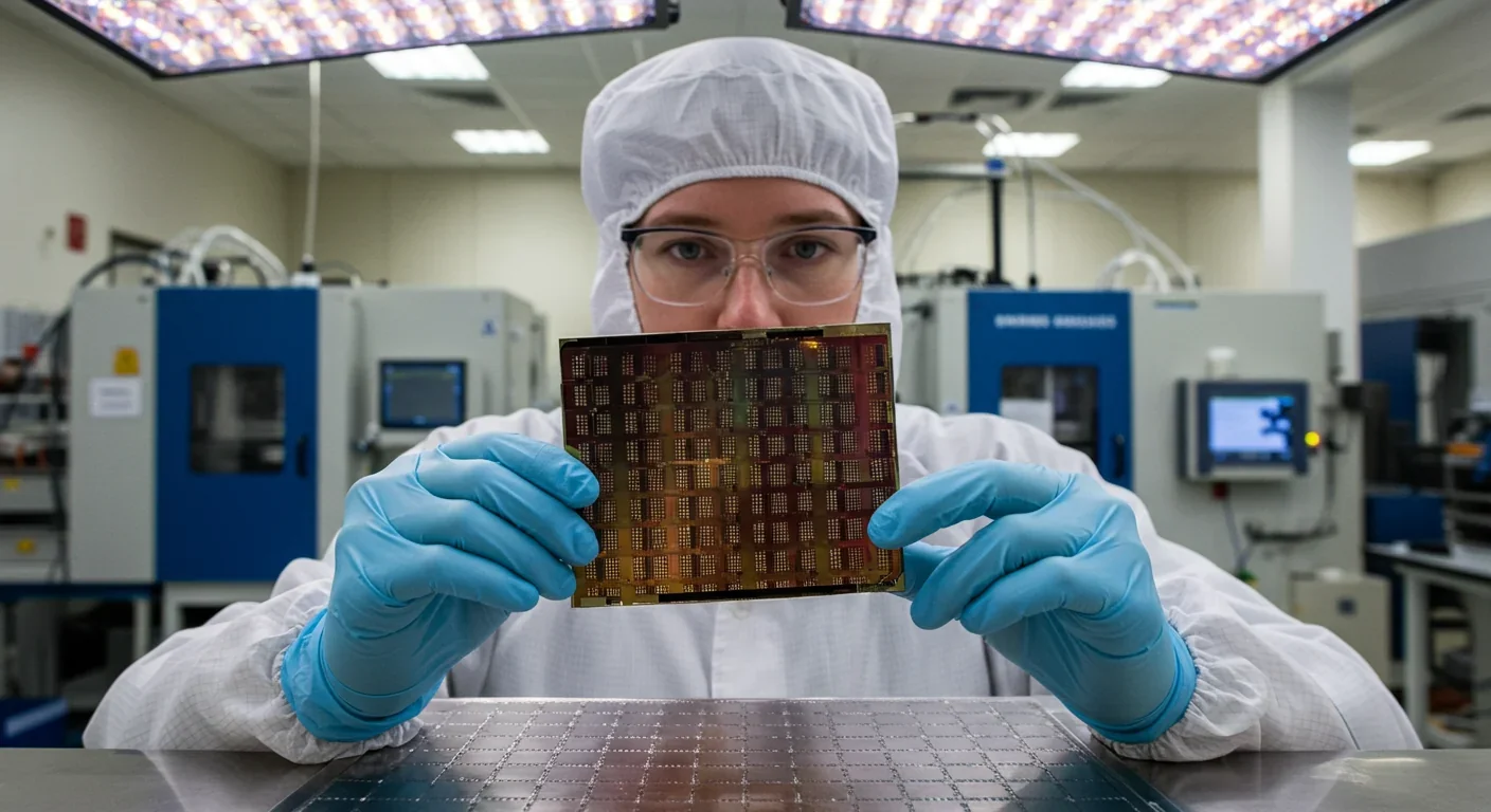
In laboratories from Silicon Valley to Shandong, researchers are fabricating a component that shouldn't exist according to classical circuit theory—yet it's poised to obsolete the entire memory hierarchy that has defined computing for seventy years. The memristor, first predicted in 1971 but realized only in 2008, doesn't just store data or process information: it does both simultaneously, in the same nanoscale device. By 2034, this technology could command an $11 billion market, fundamentally altering how AI models train, how autonomous vehicles react, and how data centers consume power. What makes a resistor "remember," and why does that memory threaten to collapse the boundary between storage and CPU?
When Leon Chua at UC Berkeley mathematically predicted the memristor in 1971, he identified a missing fundamental circuit element—a fourth companion to the resistor, capacitor, and inductor. For decades it remained theoretical, a curiosity in textbooks. Then in 2008, HP Labs fabricated a working device: a 50-nanometer film of titanium dioxide sandwiched between platinum electrodes. Apply voltage in one direction and oxygen vacancies drift through the oxide, lowering resistance; reverse the voltage and the vacancies retreat, raising resistance again. Remove power entirely and the resistance state persists indefinitely—the device "remembers" its history.
This non-volatile resistance switching unlocked a capability no previous component offered: analog, incremental tuning of conductance that survives power loss. A single memristor can store not just binary 0 or 1, but sixteen distinct states (4-bit resolution), and retain them for ten years at room temperature without refresh. Researchers at institutions worldwide have since demonstrated endurance exceeding 10⁵ write cycles and retention beyond 10⁵ seconds, with switching voltages as low as 1.36 V and latencies under 30 nanoseconds.
The implications ripple far beyond component catalogs. Traditional computing shuttles data between separate memory chips and processing cores—the infamous von Neumann bottleneck that throttles AI training and starves CPUs of bandwidth. Memristors perform in-memory computing: arrange them in a crossbar array, encode neural network weights as conductance values, and the physics of Ohm's law executes matrix–vector multiplication in a single timestep. No data movement. No fetch-decode-execute cycle. Just massively parallel analog computation at the speed of electron drift.
IBM's NorthPole chip, leveraging phase-change memristors in 256×256 arrays, recently demonstrated inference on a 3-billion-parameter model 46.9 times faster and 72.7 times more energy-efficient than the leading GPU. That performance gap isn't incremental—it's architectural. The memristor collapses storage and computation into one physical element, sidestepping the bottleneck entirely.
Every leap in computing rests on a prior revolution in materials. The telegraph required conductive wire; vacuum tubes demanded high-purity glass; transistors needed crystalline silicon. Each advance took decades to mature from laboratory curiosity to mass production. The memristor follows this arc, but with a twist: its closest historical analogue is magnetic core memory from the 1950s—tiny ferrite rings threaded with wires, storing bits as magnetic orientation. Core memory was non-volatile, radiation-hard, and required no refresh, but it was bulky and slow. Semiconductor DRAM and flash eclipsed it by the 1970s, trading non-volatility for density and speed.
Now the pendulum swings back. Modern computing demands persist data without power, access it faster than DRAM, and write it more often than flash—a combination no single technology delivers. DRAM loses data in milliseconds without refresh; flash wears out after tens of thousands of writes; hard drives can't match semiconductor speed. For fifty years, architects patched over these gaps with caches, buffers, and hierarchies. Memristors promise to eliminate the patchwork.
History also teaches caution. In 2015, Intel and Micron launched 3D XPoint (Optane), a bulk-switching, non-volatile memory using Ovonic Threshold Switches and chalcogenide glass. Early Optane SSDs delivered 95,000 IOPS with 9-microsecond latency—two to three times faster than PCIe NAND—and the technology seemed poised to disrupt data centers. Yet by 2022, both companies had discontinued it, citing insufficient demand and production costs. The lesson: even proven technology fails if manufacturing yield, price per gigabyte, or ecosystem integration lags.
Memristors must learn from Optane's fate. Materials—whether titanium dioxide, tantalum oxide, hafnium oxide, or silver-ion electrolytes—must integrate into existing CMOS fabs without exotic equipment. Process temperatures must stay below 400°C to avoid damaging underlying transistors. Device-to-device variability, filament instability, and write endurance must reach or exceed flash benchmarks. And critically, software stacks, compilers, and APIs must support in-memory computing primitives, or the hardware advantage evaporates.
At its core, a memristor operates through controlled filament formation. In resistive RAM (ReRAM), a thin insulating oxide separates two metal electrodes. Apply sufficient voltage and metal ions (commonly copper or silver) migrate from one electrode into the oxide, forming a conductive filament that bridges the gap—switching the device from high resistance (gigaohms) to low resistance (kilohms). Reverse the voltage and the filament partially dissolves, raising resistance again. The filament's geometry—its diameter, length, and branching—encodes the analog conductance value.
Crucially, this switching is non-volatile and incremental. Small voltage pulses grow the filament step by step, enabling multi-level states. A 2025 study of Cu:Te/TaOx memristors achieved sixteen distinct conductance levels by adjusting compliance current during the SET operation, with each level stable for over 100 seconds. Because the filament forms preferentially at grain boundaries and nucleation sites—such as gold nanoseeds in CuO devices—engineers can tune switching thresholds by controlling material microstructure.

This granular control transforms the memristor into an analog synapse. In a biological brain, synaptic strength varies continuously; in a digital neural network, weights are quantized to 8, 16, or 32 bits. Memristors bridge the gap, storing weights as physical conductance and updating them with voltage pulses—no digital-to-analog converter required. When arranged in a crossbar, input voltages applied to rows generate currents through each memristor; Kirchhoff's law sums these currents at column outputs, completing a matrix multiplication in one step. This is physics-native computing: the analog multiply-accumulate happens in the device itself, not in a separate ALU.
The power savings are staggering. SRAM-based AI accelerators dissipate watts shuttling data between memory and MAC units; memristor crossbars perform the same operation in picojoules, with energy dominated by wire capacitance rather than logic switching. IBM's Hermes chip, with 64 cores of 256×256 phase-change memristor arrays, achieves 1 GFLOPS per watt—an order of magnitude better than CPU or GPU. And because memristors are passive devices with near-zero leakage, idle power approaches zero.
Yet analog computing carries intrinsic noise. Memristors exhibit read noise (random conductance fluctuations during measurement) and write variability (inconsistent filament growth). Phase-change memory (PCM) shows ~2% read noise per programmed conductance; ReRAM manages ~1%. At the array level, IR drop—voltage sag across high-conductance states—limits crossbar size to hundreds of devices unless selectors or sense amplifiers compensate. Bit-slicing (using multiple memristors per weight) can average out noise, but with diminishing returns beyond eight devices. The engineering challenge: exploit analog efficiency while maintaining digital reliability.
The memristor arrives as humanity confronts an unsustainable trajectory. Global data-center electricity consumption exceeded 200 terawatt-hours in 2023—roughly 1% of worldwide generation—and AI training runs now require megawatts for weeks. GPT-3's training emitted as much CO₂ as five cars over their lifetimes; GPT-4's impact remains undisclosed but is presumed far higher. As models scale to trillions of parameters, the energy cost of shuffling weights between DRAM and GPU threatens to make further progress economically and environmentally untenable.
Memristor-based in-memory computing offers a lifeline. By eliminating data movement, neuromorphic chips could reduce AI inference energy by two orders of magnitude while accelerating throughput proportionally. That means the same model runs faster, cheaper, and cooler—or equivalently, a data center handles ten times the workload without adding capacity. For hyperscalers like Google, Amazon, and Microsoft, whose cloud margins hinge on performance per watt, the incentive is existential.
Beyond data centers, the technology cascades into transportation, healthcare, and communication. Autonomous vehicles demand real-time sensor fusion and decision-making with milliwatt power budgets; memristor accelerators can execute neural networks locally, without cloud latency or cellular bandwidth. Wearable medical devices—such as epilepsy monitors using reservoir computing on four-memristor bridge synapses—can detect seizures in wrist-worn accelerometers, enabling interventions before consciousness is lost. Smartphones and edge devices gain the ability to run large language models on-device, preserving privacy and eliminating server round-trips.
Yet this transition reshapes labor and skill. Software engineers trained on von Neumann architectures must learn to program dataflow graphs, asynchronous spikes, and analog tolerances. Hardware designers accustomed to deterministic logic must embrace stochastic devices and statistical guarantees. Entire industries—DRAM fabs, flash controllers, cache coherence protocols—face obsolescence. The social compact that stable technology affords stable careers fractures anew.
History rhymes. The mechanization of agriculture displaced farmhands into factories; the automation of factories is now displacing workers into services. Each wave provokes dislocation, then (eventually) prosperity for those who adapt. Memristors are poised to trigger the next wave: the mechanization of thought. If in-memory computing makes AI inference ubiquitous and near-free, then every device, every sensor, every transaction embeds intelligence. The line between tool and agent blurs. What happens when your refrigerator, your car, and your thermostat each possess the reasoning capacity of a college intern?
Memristors deliver three core advantages that existing memory cannot match: non-volatility, analog tunability, and in-memory computation. Non-volatility means instant-on systems with zero standby power—smartphones that wake in milliseconds, laptops that never "sleep," servers that survive power outages without data loss. Analog tunability means dense, multi-bit storage without stacking transistors—16 states per cell instead of 1, quadrupling capacity in the same footprint. And in-memory computation means collapsing the memory hierarchy into a single layer, eliminating the caches, buses, and controllers that consume half a processor's die area and power budget.
Consider the automotive sector, where over-the-air updates and adaptive cruise control demand memory that endures temperature extremes, radiation, and millions of write cycles. MRAM (magnetoresistive RAM) already ships in automotive microcontrollers for its endurance and speed; ReRAM and memristors promise even higher density and lower cost. Panasonic's 12-Mbit ReRAM, packaged in a 2×3 mm footprint, targets wearables and hearing aids—devices where battery life is paramount and space is scarce. Fujitsu, Crossbar, and Weebit Nano are racing to scale similar designs to gigabyte capacities.
In high-performance computing, memristor accelerators address the memory wall that stalls supercomputers: processors idle while waiting for data. By co-locating compute with storage, hybrid CPU-memristor systems can dynamically allocate tasks—CMOS cores handle control flow and branching; memristor arrays handle matrix-heavy inference. IMEC's OxRAM neuromorphic chip demonstrated self-learning by composing a 30-second music clip from four flute minuets, proving that memristors can both store and adapt weights on-chip. Intel's Loihi chip, though using CMOS neurons, pioneered the asynchronous, event-driven computing paradigm that memristors excel at: sparse, low-power activation modeled after biological spiking.
The density gains are equally transformative. Passive crossbar memristor arrays achieve 4F² per bit (where F is the minimum lithography feature size), compared to 6F² for DRAM and 4F² for single-level NAND flash. But memristors support multi-level storage (4 bits per cell) without additional transistors, effectively multiplying density by four. Stack multiple layers using through-silicon vias, and terabyte-class memories fit in credit-card form factors. Crossbar Inc. prototyped a three-layer silver-ion ReRAM with a theoretical 1 TB capacity—though manufacturing yield and endurance remain unproven at scale.
Even more compelling: memristors enable mixed-mode in-memory computing, where the same crossbar array performs both analog matrix multiplication and digital logic operations. Researchers demonstrated Boolean gates (AND, OR, XOR) directly within memristive networks, orchestrated by adaptive control algorithms that tune resistance states on the fly. This dual-mode capability unlocks logic-in-memory, a decades-old dream now approaching reality. Imagine a processor where every cache line is also an ALU, where fetching data inherently transforms it. The performance potential is exponential.
No technology is a panacea. Memristors confront formidable obstacles that have stalled commercialization for over a decade. Device variability tops the list: filament formation is inherently stochastic, governed by atomic-scale defects, grain boundaries, and thermal noise. Even nominally identical devices on the same wafer exhibit SET voltages that vary by ±40% and conductance distributions spanning an order of magnitude. While bit-slicing and error-correcting codes can compensate, they erode the density and energy advantages.
Write endurance remains a second barrier. Flash memory endures 10⁴ to 10⁵ program-erase cycles; DRAM effectively unlimited (but volatile). Memristors fall somewhere in between: ReRAM prototypes demonstrate 10⁵ cycles, PCM reaches 10⁸, but both degrade as filaments fracture or crystalline phases irreversibly mix. For AI inference (read-heavy workloads), this suffices; for training (write-heavy), it's marginal. The dual-mode ferroelectric-memristor stack from CEA-Leti addresses this by using ferroelectric capacitors for frequent updates and memristors for inference, but the approach requires precise electrical "forming" and adds fabrication complexity.

Thermal management plagues high-density arrays. Switching a memristor dissipates picojoules, but multiply by millions of devices toggling in parallel and local hotspots emerge, accelerating aging and crosstalk. PCM is especially vulnerable: switching relies on melting and quenching chalcogenide glass, a process that generates significant heat. Passive cooling suffices for small arrays; megabit-scale crossbars may require active thermal control, negating some power advantage.
Integration with CMOS presents a manufacturing Rubicon. Most memristors require back-end-of-line (BEOL) fabrication—deposited atop finished transistors—to avoid thermal budget violations. This constrains materials to those stable below 400°C and compatible with aluminum or copper interconnects. Titanium, tantalum, and hafnium oxides meet these criteria; silver and copper electrolytes are riskier (ion migration can poison transistors). Foundries like TSMC, Samsung, and Intel have not yet standardized memristor processes, leaving each adopter to custom-engineer integration—expensive and time-consuming.
Yield and defect density compound the challenge. A 2025 wafer-scale memristor crossbar study achieved 95% device yield on 4-inch wafers—impressive for research, but commercial DRAM fabs target 99.9%. Every defect in a crossbar corrupts an entire row or column unless redundancy or remapping compensates. Rabbit-ear electrode defects, voltage drops from IR sag, and sneak-path currents (unintended conductance through neighboring cells) all demand careful design: back-filled electrodes, hexagonal line geometries, and selector devices (transistors or threshold switches) that isolate cells. Each mitigation adds area and complexity.
Finally, lack of industry standards stalls ecosystem adoption. Without standardized APIs for memristor programming, compilers cannot optimize code; without standardized electrical interfaces, accelerators cannot plug into existing systems. Synopsys offers RRAM and MRAM IP compilers, but coverage is fragmented. Software frameworks like IBM's Analog Hardware Acceleration Kit simulate memristor arrays for PyTorch, but real-world deployment lags. The gap between research prototype and product-ready module remains measured in years, not quarters.
The memristor market landscape is fragmented and fiercely competitive. North America holds the largest market share, driven by R&D powerhouses (Stanford, MIT, IBM Research) and venture capital (Rain Neuromorphics raised $25 million in 2023 to layer memristor circuits atop silicon wafers). Hewlett Packard Enterprise pioneered titanium dioxide devices; Crossbar Inc. developed silver-ion 1T1R ReRAM on a 40-nm process at SMIC, with a roadmap to 16-nm, four-layer stacks targeting 32 GB. Intel's Loihi neuromorphic chip and IBM's NorthPole inference processor both incorporate or interface with non-volatile memory arrays, signaling major players' commitment.
Asia-Pacific is projected to grow fastest, with a CAGR exceeding 22% through 2030. China's Shandong University leads research into low-power memristors for edge AI. Japan's Panasonic shipped the world's first commercial ReRAM in 2013—an 8-bit microcontroller with embedded 180-nm ReRAM—and has since progressed to 40-nm devices targeting 2025 retail. Fujitsu launched a 12-Mbit ReRAM for wearables (smartwatches, hearing aids) in a 2×3 mm package. South Korea's Samsung and SK Hynix, dominant in DRAM and NAND, are hedging with MRAM and ReRAM R&D, though commercial memristor products remain undisclosed.
Europe contributes critical research: IMEC (Belgium) demonstrated the first self-learning OxRAM chip that composed music; CEA-Leti (France) fabricated the unified ferroelectric-memristor stack on 130-nm CMOS. Weebit Nano (Australia/Israel) licenses ReRAM IP emphasizing CMOS compatibility—using standard materials and equipment to lower foundry integration barriers.
Yet the market remains nascent. Valued at $205 million in 2023, memristors are projected to reach $9.5–$11.25 billion by 2032–2034, implying a CAGR of 51–54%. For context, the broader non-volatile memory (NVM) market stood at $64.55 billion in 2023, growing at 9% CAGR; memristors' faster growth reflects a smaller base and higher risk. Nanoionic memristors—operating via ion migration—are the fastest-growing segment (>57% CAGR), prized for fast switching and endurance.
Investment trends reveal priorities: AI accelerators, automotive electronics, and IoT edge devices command the highest interest. Automotive and aerospace, where reliability and radiation tolerance are paramount, account for top-tier growth. Data centers, driven by exploding AI workloads, represent the largest addressable market. Consumer electronics (smartphones, wearables) lag due to cost sensitivity and the dominance of incumbent DRAM/NAND ecosystems.
Competition from mature NVM technologies looms. MRAM delivers near-DRAM speed, high endurance, and is already shipping in automotive MCUs and cache replacement; Samsung, Everspin, and Micron are scaling production. 3D XPoint, though discontinued by Intel and Micron, proved that alternative memory architectures can achieve commercial scale—and also that market fit and manufacturing cost matter as much as raw performance. FeRAM (ferroelectric RAM) offers low power and instant writes but limited density. Memristors must outcompete on density, cost per bit, and ecosystem integration, or risk the fate of ReRAM—perpetually "promising" but never dominant.
As memristors mature, individuals and organizations face strategic choices. For engineers and researchers, the shift demands fluency in analog circuit design, stochastic computing, and neuromorphic algorithms. Universities are slow to update curricula; online courses, IEEE workshops, and open-source simulation tools (like IBM's AI HW Kit) fill the gap. Hands-on experience with commercial memristor dev kits—Knowm Inc. offers bridge-synapse boards for reservoir computing—accelerates learning.
Product managers and entrepreneurs should monitor integration timelines and cost trajectories. Early adopters will target niches where memristors' strengths (non-volatility, energy efficiency, in-memory compute) outweigh immaturity: space systems (radiation tolerance), medical implants (ultra-low power), edge AI (local inference without cloud). Mass-market penetration—smartphones, laptops, servers—awaits standardized foundry processes, multi-gigabyte capacities, and price parity with DRAM or NAND. Industry roadmaps suggest 2027–2030 for embedded memory in MCUs; 2030–2035 for standalone memristor modules competing with DDR5.
Investors face a classic innovator's dilemma: incumbents (Samsung, Micron, SK Hynix) possess manufacturing scale but risk channel conflict (memristors cannibalize DRAM/NAND revenue); startups (Crossbar, Weebit, Rain Neuromorphics) are nimble but capital-starved and lack fabs. The winning formula may be partnerships—startups license IP, incumbents provide foundry access—but execution is fraught. History suggests that the first to achieve high-yield, high-volume production at cost parity will capture the market, regardless of technical elegance.
Policymakers should recognize memristors as dual-use technology: enabling both civilian AI (healthcare diagnostics, climate modeling) and military systems (autonomous drones, encrypted communications). Export controls, technology transfer restrictions, and domestic manufacturing incentives (such as the U.S. CHIPS Act's $52 billion) will shape which nations lead. China's state-backed investments in Shandong and elsewhere; Europe's emphasis on open research consortia; and America's venture-capital-driven model represent divergent paths to the same goal.
On a personal level, digital literacy must expand to encompass hardware awareness. As AI inference moves from cloud to edge, users will encounter "intelligence" in thermostats, refrigerators, and wearables—devices that learn behavior, adapt autonomously, and operate offline. Understanding the limitations (training data bias, adversarial vulnerability) and capabilities (real-time adaptation, privacy-preserving local compute) of memristor-powered AI empowers informed consent and responsible use.
The skills worth cultivating: systems thinking (how memory, compute, and algorithms co-evolve), energy literacy (recognizing power-performance tradeoffs), and adaptive learning (the pace of hardware change now rivals software). Those who master these thrive; those who don't risk obsolescence.
The memristor is more than a circuit component—it's a pivot point in civilization's relationship with information. For a century, we've organized knowledge into discrete silos: storage in one place, processing in another, transmission via a third. The von Neumann architecture codified this separation, and every CPU, GPU, and data center since has reinforced it. Memristors propose a radically different model: computation as an emergent property of storage itself. Data doesn't travel to a processor; the processor is wherever the data resides.
This collapse has precedent. The printing press collapsed the scribe and the library into a distributed network of readers. The internet collapsed the broadcaster and the audience into a web of peers. Memristors threaten to collapse the memory and the CPU, dissolving the boundary that has structured hardware design for seventy years. When that boundary vanishes, so do the constraints it imposed—and the mental models we've built atop it.
Adapting will be wrenching. Programmers must unlearn sequential thinking; architects must abandon caches and buses; investors must revalue supply chains. But the reward—a computing paradigm that mirrors biological brains in efficiency and parallelism—could be existential. If AI demands exponentially more compute, and conventional scaling hits physical limits, memristors may be the only path forward that doesn't require exponentially more power plants.
Yet we should approach with humility. Every revolutionary technology carries unintended consequences. Electricity democratized industry—and enabled factory accidents. Automobiles liberated travel—and choked cities with smog. Social media connected billions—and weaponized outrage. Memristors will empower edge AI, slash energy use, and unlock new applications we can't yet imagine. They will also concentrate power in those who control the foundries, the algorithms, and the data. They will make surveillance cheaper, persuasion subtler, and autonomy more fragile.
The technology is coming. The question isn't whether memristors will redefine computing—it's whether we'll design the transition to amplify human agency or erode it. Will memristor-powered AI serve as a tool we wield, or an infrastructure we inhabit? Will local inference preserve privacy, or enable manipulation too fast to detect? Will in-memory computing democratize intelligence, or centralize it in those with capital to fabricate trillion-device arrays?
These aren't technical questions—they're political, ethical, and deeply personal. And the answers we give, in the next decade, will shape the century to follow. The memristor remembers. What will it remember about us?
Recent breakthroughs in fusion technology—including 351,000-gauss magnetic fields, AI-driven plasma diagnostics, and net energy gain at the National Ignition Facility—are transforming fusion propulsion from science fiction to engineering frontier. Scientists now have a realistic pathway to accelerate spacecraft to 10% of light speed, enabling a 43-year journey to Alpha Centauri. While challenges remain in miniaturization, neutron management, and sustained operation, the physics barriers have ...

Epigenetic clocks measure DNA methylation patterns to calculate biological age, which predicts disease risk up to 30 years before symptoms appear. Landmark studies show that accelerated epigenetic aging forecasts cardiovascular disease, diabetes, and neurodegeneration with remarkable accuracy. Lifestyle interventions—Mediterranean diet, structured exercise, quality sleep, stress management—can measurably reverse biological aging, reducing epigenetic age by 1-2 years within months. Commercial ...

Data centers consumed 415 terawatt-hours of electricity in 2024 and will nearly double that by 2030, driven by AI's insatiable energy appetite. Despite tech giants' renewable pledges, actual emissions are up to 662% higher than reported due to accounting loopholes. A digital pollution tax—similar to Europe's carbon border tariff—could finally force the industry to invest in efficiency technologies like liquid cooling, waste heat recovery, and time-matched renewable power, transforming volunta...

Humans are hardwired to see invisible agents—gods, ghosts, conspiracies—thanks to the Hyperactive Agency Detection Device (HADD), an evolutionary survival mechanism that favored false alarms over fatal misses. This cognitive bias, rooted in brain regions like the temporoparietal junction and medial prefrontal cortex, generates religious beliefs, animistic worldviews, and conspiracy theories across all cultures. Understanding HADD doesn't eliminate belief, but it helps us recognize when our pa...

The bombardier beetle has perfected a chemical defense system that human engineers are still trying to replicate: a two-chamber micro-combustion engine that mixes hydroquinone and hydrogen peroxide to create explosive 100°C sprays at up to 500 pulses per second, aimed with 270-degree precision. This tiny insect's biochemical marvel is inspiring revolutionary technologies in aerospace propulsion, pharmaceutical delivery, and fire suppression. By 2030, beetle-inspired systems could position sat...

The U.S. faces a catastrophic care worker shortage driven by poverty-level wages, overwhelming burnout, and systemic undervaluation. With 99% of nursing homes hiring and 9.7 million openings projected by 2034, the crisis threatens patient safety, family stability, and economic productivity. Evidence-based solutions—wage reforms, streamlined training, technology integration, and policy enforcement—exist and work, but require sustained political will and cultural recognition that caregiving is ...
Every major AI model was trained on copyrighted text scraped without permission, triggering billion-dollar lawsuits and forcing a reckoning between innovation and creator rights. The future depends on finding balance between transformative AI development and fair compensation for the people whose work fuels it.

Loading featured articles...