How Transformers Replaced Word2Vec in NLP
How Transformers Replaced Word2Vec in NLP

How AlphaGo Mastered Go Using Reinforcement Learning

Zero-Knowledge Proofs: Prove Identity Without Data Exposure
How Tensor Cores Power Today's AI Breakthroughs
The Quantum Internet Is Coming: Entanglement-Based Networks
Vision Transformers vs CNNs: The Computer Vision Revolution
TL;DR: Photonic processors use light instead of electrons to process data, promising 25-100x better AI performance per watt. Hybrid systems shipping 2025-2027 will target data centers, while all-optical general-purpose computers remain beyond 2028.
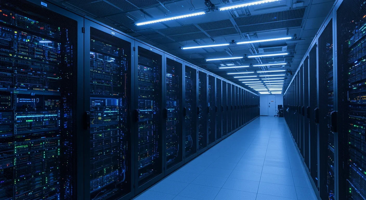
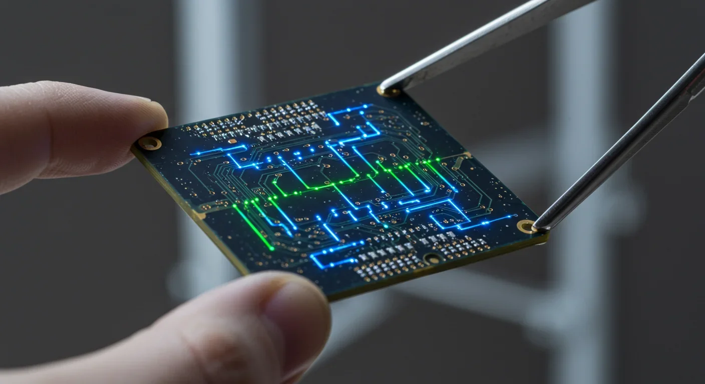
Imagine a computer chip where information travels at, quite literally, the speed of light. Not through electrons crawling along silicon pathways, but through photons—particles of light—zipping through optical waveguides carved into silicon. This isn't science fiction or distant speculation. It's happening right now in labs across the world, and the performance numbers are staggering.
Photonic computing—using light instead of electricity to process information—promises speed improvements that sound almost absurd. Some researchers claim 1,000 times faster than today's silicon chips. Others report 25 to 100 times better performance than high-end GPUs on specific tasks. Meanwhile, startups like Lightmatter have raised hundreds of millions to commercialize the technology, and tech giants from Intel to Microsoft are quietly building their own photonic prototypes.
So what's real, and what's hype? More importantly, when will you actually be able to buy one of these light-based processors?
The fundamental shift is deceptively simple: replace electrons with photons. In conventional processors, billions of transistors switch electrical currents on and off to represent ones and zeros. This approach has powered computing for seven decades, but it's hitting walls. Transistors can't get much smaller without quantum effects causing chaos. Heat buildup limits how fast chips can run. And crucially, optoelectronic devices waste 30% of their energy just converting electrical signals into optical signals and back for data transmission.
Photonic processors skip that conversion entirely. Light pulses carry data through silicon waveguides—essentially microscopic fiber-optic cables etched directly onto chips. These photons can be modulated, routed, and processed using components like ring resonators, Mach-Zehnder interferometers, and optical switches. Since photons don't interact with each other the way electrons do, you can send multiple wavelengths of light through the same waveguide simultaneously—a trick called wavelength-division multiplexing that effectively gives you hundreds of parallel data channels for free.
The physics gets even better. Photons travel at roughly 200,000 kilometers per second in silicon, compared to electrons moving at a tiny fraction of that speed. They generate almost no heat during transmission. And because light beams can cross without interfering, photonic circuits can stack connections in ways that would cause catastrophic short circuits in electronic chips.
Photons travel 200,000 km/s in silicon and generate almost no heat, enabling circuit designs impossible with electrons that would short-circuit if they crossed paths.
This isn't just theory. Researchers have built working prototypes. The question is whether they can scale.
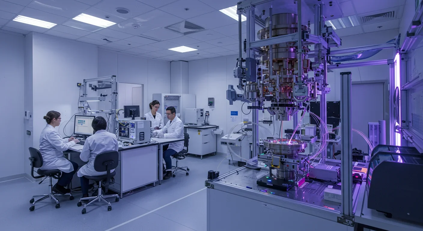
For years, photonic computing was stuck in a frustrating loop. Labs would demonstrate impressive individual components—an optical switch here, a photonic memory cell there—but nobody could integrate them into a complete, practical processor. The challenge was building an optical equivalent of the transistor: something small, fast, low-power, and mass-producible.
Then came a series of breakthroughs between 2023 and 2025 that cracked the problem.
In October 2024, researchers at the University of Pittsburgh announced they'd created a photonic memory cell with performance that sounded almost fictional: 2.4 billion switching cycles, nanosecond-speed operation, and multibit storage in a single device. It used magneto-optical effects in cerium-doped yttrium iron garnet (Ce:YIG) integrated directly on silicon. Critically, it could be programmed with standard CMOS circuits, meaning it would work with existing chip manufacturing infrastructure.
Around the same time, researchers in China demonstrated ultra-compact photonic AI chips with parallelism levels exceeding 100—meaning they could process over 100 operations simultaneously. In Switzerland, scientists achieved wavelength-division multiplexing with 100 independent data channels on a single photonic chip, essentially multiplying bandwidth by a factor of 100 without adding more physical space.
Perhaps most importantly, labs across the globe figured out how to fabricate low-loss optical components at scale. Silicon nitride waveguides now achieve losses below 0.1 dB per centimeter, meaning light can travel relatively long distances on-chip without significant signal degradation. That's the kind of unglamorous engineering advance that makes the difference between a clever demo and a real product.
"We demonstrate a unique solution that addresses current limitations of optical memory that have yet to combine non-volatility, multibit storage, high switching speed, low switching energy, and high endurance in a single platform."
— Nathan Youngblood, University of Pittsburgh
These breakthroughs share something in common: they're all compatible with silicon photonics, the manufacturing approach that leverages existing semiconductor fabrication plants. You're not building an entirely new industry from scratch—you're adapting one that already produces billions of chips annually.
The 1,000x speed claim sounds like marketing exaggeration, and in many cases, it is. But dig into the specifics, and you find areas where photonic processors genuinely dominate.
Matrix multiplication for AI workloads is the killer application. Deep learning models spend most of their time multiplying massive matrices together. Photonic tensor cores—specialized optical circuits designed for this exact task—can perform these calculations by encoding numbers as light intensities and using interference patterns to multiply them. Because this happens at the speed of light with minimal energy loss, the theoretical speedup is enormous. Real-world tests show 25 to 100 times better performance per watt than GPUs on AI inference tasks.
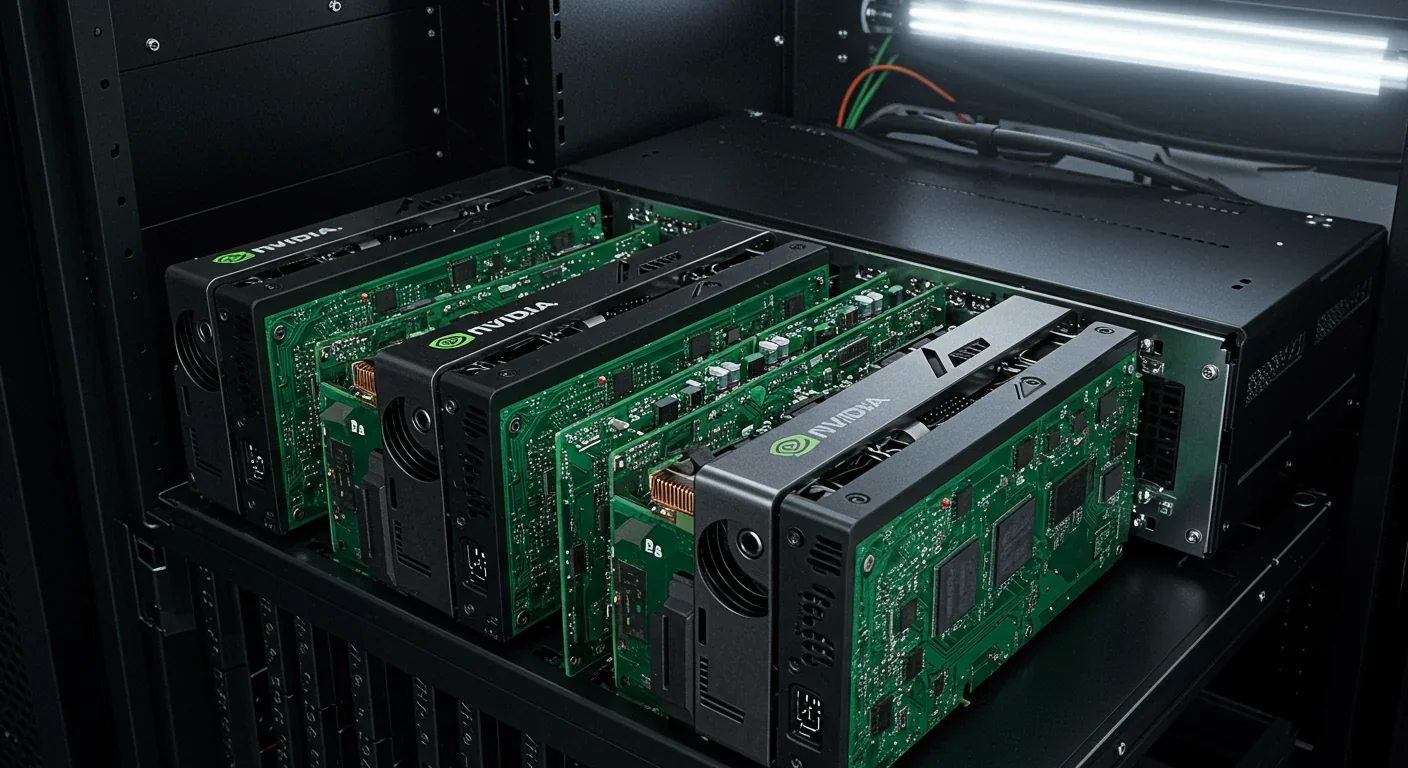
Data center interconnects are another sweet spot. Modern data centers move petabytes of information between servers, and the electrical-to-optical conversions at every step waste massive amounts of power. Intel's integrated optical I/O chiplet and competitors like Avicena's LightBundle platform promise to move data at terabit-per-second speeds using a fraction of the power. When you're Google or Meta running millions of servers, those efficiency gains translate to tens of millions of dollars in electricity savings annually.
Neuromorphic computing—building chips that mimic how brains process information—also benefits. Photonic neuromorphic processors can implement neural networks where neurons are represented by optical components and synapses by tunable interference patterns. Research teams have demonstrated beyond-terabit-per-second processing for certain neural network architectures, though these remain experimental.
But here's the catch: photonic processors aren't general-purpose computers. They excel at specific tasks—linear algebra, signal processing, certain AI models—but struggle with the branching logic and irregular memory access patterns that CPUs handle effortlessly. An all-optical laptop running your email and web browser? Not happening anytime soon, probably not ever.
Walk through any major technology conference in 2025, and you'll trip over photonic computing startups. Some have raised eye-watering sums.
Lightmatter, founded by MIT researchers, is probably the highest-profile. They've raised over $400 million and reached a $1.2 billion valuation building hybrid photonic-electronic processors specifically for AI workloads. Their approach cleverly sidesteps the general-purpose computing problem by focusing on accelerating the matrix multiplications that AI models desperately need. They're partnering with Amkor Technology to build the world's largest 3D photonics package, integrating six photonic chips into a single massive processor.
Lightelligence, another MIT spinoff, takes a similar AI-acceleration angle. Xanadu focuses on photonic quantum computing, a different beast entirely but leveraging overlapping technology. In Europe, Arago just raised $26 million to develop photonic chips for edge AI applications, promising dramatic reductions in power consumption.
Meanwhile, the tech giants are hedging their bets. Intel demonstrated its first integrated optical I/O chiplet in early 2025. Microsoft has been exploring optical data storage through Project Silica and quietly investing in photonic interconnects for Azure data centers. IBM, traditionally conservative about new computing paradigms, has published research on photonic tensor cores and optical neural networks.
In Asia, Taiwan-backed startups are targeting cloud giants with photonic chips scheduled for 2026 launch. China's research institutions—particularly USST and SIOM—have demonstrated ultra-compact chips with extreme parallelism, though commercial products remain vaporware for now.
The photonic integrated circuit market is projected to exceed $50 billion by 2035, with compound annual growth rates above 20% through the 2030s as the technology matures.
The market projections are wild. Analysts predict the photonic integrated circuit market will exceed $50 billion by 2035. Some forecasts go higher, projecting compound annual growth rates above 20% through the 2030s.
Now for the sobering part. Despite the impressive lab results and breathless headlines, actual photonic processors you can buy and plug into a server rack? Almost none.
What's shipping today are hybrid systems—devices that use photonics for specific bottlenecks while relying on conventional electronics for everything else. Lightmatter's approach epitomizes this: photonic interconnects move data between electronic processors at light speed, and photonic accelerators handle matrix math, but control logic and memory access remain firmly electronic.
These hybrid architectures make sense. They exploit photonics' strengths while avoiding its weaknesses. The problem is they don't deliver the full 1,000x speedup that pure optical computing promises. More like 10x to 100x on specific workloads, which is still impressive but less revolutionary.
First-generation products are targeting data centers, not consumers. The photonic co-processors expected to ship in 2025-2027 will slot into high-performance computing clusters running AI training and inference. Think hyperscalers like AWS, Google Cloud, and Microsoft Azure buying thousands of units to improve the efficiency of their GPU farms. You won't find photonic chips in laptops or smartphones for at least a decade, possibly ever.
And all-optical general-purpose processors? Industry consensus puts those beyond 2028, maybe significantly beyond. The engineering challenges are brutal.
Photonic computing's dirty secret: it's really, really hard to build.
Integration complexity is problem number one. Modern silicon chips pack billions of transistors into a fingernail-sized die. Photonic components are much larger—a single ring resonator might occupy the space of thousands of transistors. You simply can't achieve the same integration density, which limits the computational power you can squeeze onto a chip.
Nonlinearity bottlenecks create another headache. Electronic transistors have strong nonlinear responses—small changes in input voltage create large changes in current flow. That's what lets them act as switches and logic gates. Optical materials have much weaker nonlinear effects, meaning you need longer interaction lengths or higher light intensities to achieve similar switching behavior. Both increase chip size and power consumption, eroding photonics' advantages.
"The performance of optical logic gates hinges on the strength of nonlinear optical effects, which are typically weak; large-scale integration therefore requires materials with very high nonlinearity and extremely low propagation losses."
— Wikipedia: Optical Computing
Light source challenges are surprisingly tricky. Electronic chips generate their own electricity from a power supply. Photonic chips need laser light, which must be generated somewhere, coupled onto the chip, split into multiple wavelengths, and kept stable. On-chip laser integration remains a major research challenge, and most current designs rely on external lasers coupled through optical fibers—not exactly elegant or scalable.
Manufacturing scalability worries investors and engineers alike. Silicon chip fabrication is a $500+ billion global industry with decades of optimization. Photonics fabrication is projected to mature between 2026 and 2028, meaning it's years behind in manufacturing know-how. Yield rates—the percentage of chips that work correctly—are lower for photonics, driving up costs. Until dedicated photonics fabs reach the scale and efficiency of silicon foundries, prices will remain prohibitive for most applications.
Testing and debugging create headaches because you can't just probe optical signals with an oscilloscope the way you can with electrical signals. Silicon photonics raises new test challenges that require entirely new equipment and methodologies. When a photonic chip fails, figuring out why is often a nightmare.
Despite the challenges, photonic computing is finding its niches—and those niches are enormous markets.
AI inference at the edge is heating up. Running neural network models on phones, autonomous vehicles, and IoT devices devours battery power. Photonic chips that can perform inference at a fraction of the energy cost could enable always-on AI capabilities that are currently impossible. Arago's $26 million funding round specifically targets this market, promising 10x power efficiency improvements for edge AI workloads.
Data center interconnects might be photonics' killer app. As AI models grow larger, they're split across hundreds or thousands of GPUs that must communicate constantly. The bandwidth between chips is becoming the bottleneck. Intel's optical I/O chiplet and similar technologies from Ayar Labs promise to eliminate that bottleneck, enabling massively parallel AI training that's currently impractical.
Scientific computing has always been an early adopter of new architectures. Simulating quantum systems, protein folding, climate models—these tasks involve massive matrix operations that photonic accelerators could handle brilliantly. National labs and research universities are likely to be early customers, providing revenue and real-world testing grounds for first-generation products.
Telecommunications infrastructure is quietly integrating photonics already. Co-packaged optics—putting photonic transceivers directly inside networking switches rather than as separate pluggable modules—is rolling out in 5G networks and hyperscale data centers. This isn't photonic computing per se, but it's the same underlying technology, and the deployment is driving manufacturing scale-up that benefits the computing side.
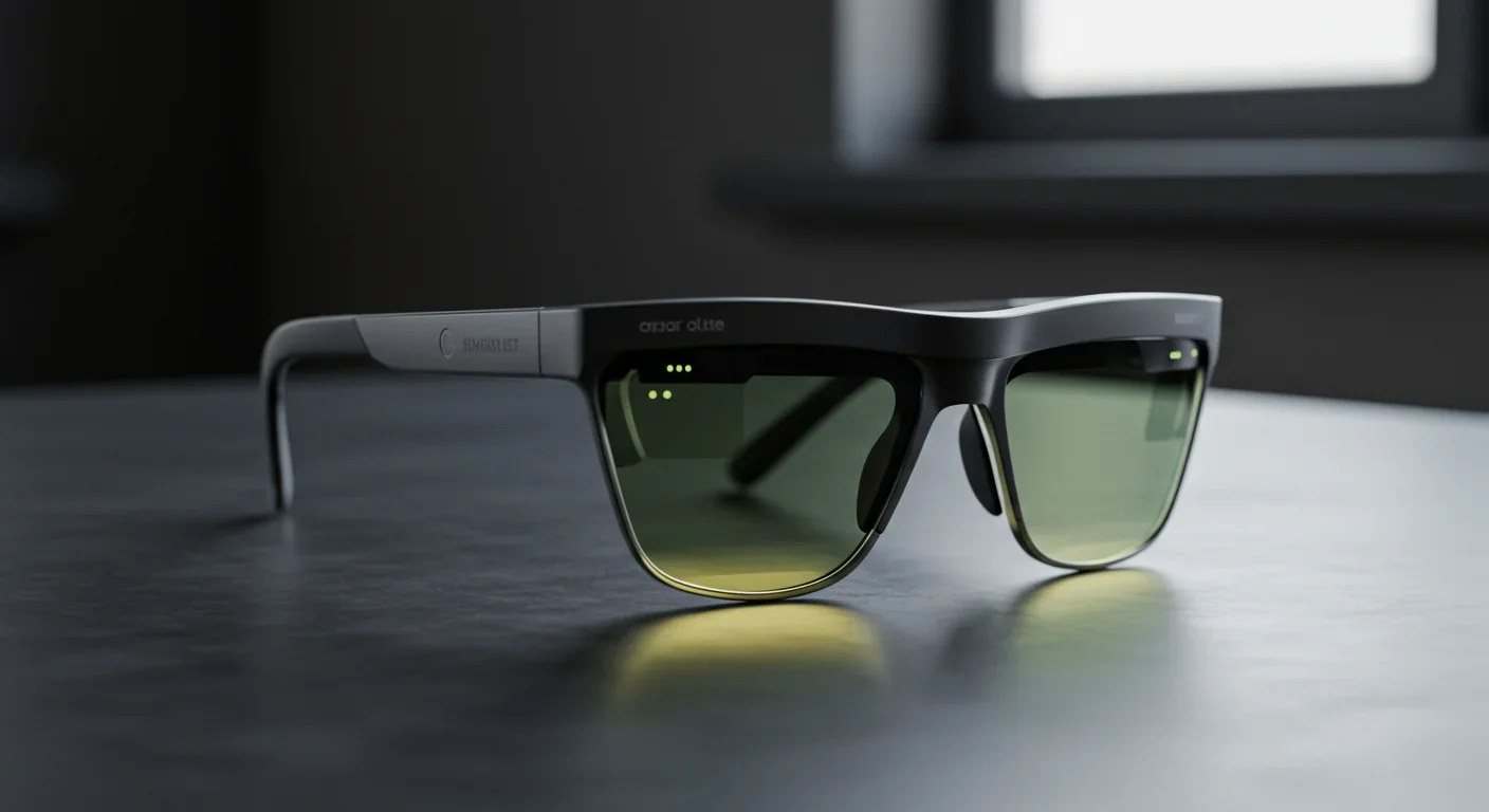
Augmented and virtual reality could benefit enormously. AR glasses need to process huge amounts of visual data in real-time while sipping power from tiny batteries. Photonic signal processing could enable lightweight AR devices that don't overheat or die after 20 minutes.
What you won't see soon: photonic chips in general-purpose PCs, laptops, or smartphones. The economics and engineering just don't work for those applications.
Let's game out the next decade, assuming photonic computing overcomes its current hurdles and achieves even half of what proponents promise.
Energy consumption drops precipitously in data centers. If photonic AI accelerators deliver even 10x better performance per watt, the global energy footprint of artificial intelligence—currently on track to consume several percent of worldwide electricity by 2030—could be cut by more than half. That's not just a climate win; it's an economic one. Energy costs are a major expense for cloud providers, and anything that cuts the power bill by 50% is worth billions.
AI model sizes explode. Right now, training frontier AI models is limited by how many GPUs you can network together before communication overhead kills performance. With photonic interconnects providing terabit-per-second bandwidth between processors, that limit evaporates. We could see AI models with trillions or tens of trillions of parameters trained as single coherent systems, potentially unlocking capabilities that current architectures can't reach.
If photonic AI accelerators deliver even 10x better performance per watt, the global energy footprint of artificial intelligence could be cut by more than half by 2030.
New computing paradigms emerge. Photonics enables architectures that are impractical or impossible with electronics. Neuromorphic photonic systems that process information more like biological brains. Analog optical computing that trades perfect digital precision for massive parallelism and efficiency. These approaches could complement or even challenge the von Neumann architecture that's dominated computing since the 1940s.
The semiconductor landscape fractures. For 50 years, silicon CMOS has been the undisputed king, with Intel, TSMC, and Samsung leading a relatively consolidated industry. Photonics introduces new materials (indium phosphide, lithium niobate, silicon nitride), new manufacturing processes, and new design rules. Established players have advantages, but startups and challengers have more room to disrupt. The industry could become more diverse and competitive—or it could consolidate again as a few companies master the new technology.
Edge intelligence becomes ubiquitous. If photonic chips crack the edge AI efficiency problem, we enter a world where every device has genuine intelligence. Your glasses recognize faces and translate languages in real-time. Autonomous vehicles process sensor data locally without relying on cloud connectivity. Medical diagnostic devices perform sophisticated analysis at the point of care. That's not a small shift—it's a fundamental change in how computing integrates into daily life.
So where does this leave us? Is photonic computing the real deal or another overhyped technology that will spend a decade disappointing investors?
The honest answer: it's both.
The physics is real. The lab demonstrations are legitimate. The engineering progress is genuine. Photonic computing will absolutely find commercial success in specific high-value applications, particularly AI acceleration and data center interconnects. Companies investing in this technology aren't chasing vaporware.
But the breathless predictions of 1,000x faster computers replacing your laptop in five years? Pure fantasy. Photonic computing is an accelerator technology, not a replacement for conventional processors. It's more like GPUs disrupting graphics rendering in the 2000s than CPUs replacing mainframes in the 1980s.
The timeline matters immensely. Hybrid photonic-electronic co-processors are shipping now or very soon—2025 to 2027 for first-generation data center products. Standalone photonic AI accelerators will likely mature in the 2027-2030 window. All-optical general-purpose processors remain beyond 2028, possibly beyond 2035, and might never be practical for many applications.
For tech professionals, the takeaway is clear: photonic computing is transitioning from research to commercialization, but the initial products will be specialized accelerators for AI and high-performance computing, not general-purpose chips. If you're in data center infrastructure, AI development, or semiconductor design, this matters to you now. If you're building consumer electronics or enterprise software, it's something to monitor but not panic about.
For investors, the opportunity is real but the landscape is treacherous. The photonic computing market will grow substantially, but most startups will fail. The winners will be companies that focus ruthlessly on specific applications where photonics' advantages are overwhelming, rather than trying to boil the ocean with all-optical general-purpose computers.
And for the rest of us, watching this technology evolve offers a fascinating glimpse into how computing advances. The transistor didn't immediately replace vacuum tubes—it found niche applications first, then gradually displaced older technology as the economics and engineering matured. Photonic computing is following a similar path. The difference is, this time we get to watch the transition in real-time, with research papers and startup funding rounds providing a play-by-play.
The age of light-speed computing is beginning. It won't look exactly like the marketing hype promises, but it might be even more interesting for the ways it surprises us.

Curiosity rover detects mysterious methane spikes on Mars that vanish within hours, defying atmospheric models. Scientists debate whether the source is hidden microbial life or geological processes, while new research reveals UV-activated dust rapidly destroys the gas.

CMA is a selective cellular cleanup system that targets damaged proteins for degradation. As we age, CMA declines—leading to toxic protein accumulation and neurodegeneration. Scientists are developing therapies to restore CMA function and potentially prevent brain diseases.

Intercropping boosts farm yields by 20-50% by growing multiple crops together, using complementary resource use, nitrogen fixation, and pest suppression to build resilience against climate shocks while reducing costs.

Cryptomnesia—unconsciously reproducing ideas you've encountered before while believing them to be original—affects everyone from songwriters to academics. This article explores the neuroscience behind why our brains fail to flag recycled ideas and provides evidence-based strategies to protect your creative integrity.

Cuttlefish pass the marshmallow test by waiting up to 130 seconds for preferred food, demonstrating time perception and self-control with a radically different brain structure. This challenges assumptions about intelligence requiring vertebrate-type brains and suggests consciousness may be more widespread than previously thought.

Epistemic closure has fractured shared reality: algorithmic echo chambers and motivated reasoning trap us in separate information ecosystems where we can't agree on basic facts. This threatens democracy, public health coordination, and collective action on civilizational challenges. Solutions require platform accountability, media literacy, identity-bridging interventions, and cultural commitment to truth over tribalism.
Transformer architectures with self-attention mechanisms have completely replaced static word vectors like Word2Vec in NLP by generating contextual embeddings that adapt to word meaning based on surrounding context, enabling dramatic performance improvements across all language understanding tasks.

Loading featured articles...